
Bron: artikel gedeeltelijk overgenomen van blog.devops.dev
Origineel auteur: SAMUEL K. MOORE
Today at Nvidia’s developer conference, GTC 2024, the company revealed its next GPU, the B200. The B200 is capable of delivering four times the training performance, up to 30 times the inference performance, and up to 25 times better energy efficiency, compared to its predecessor, the Hopper H100 GPU. Based on the new Blackwell architecture, the GPU can be combined with the company’s Grace CPUs to form a new generation of DGX SuperPOD computers capable of up to 11.5 billion billion floating point operations (exaflops) of AI computing using a new, low-precision number format.
“Blackwell is a new class of AI superchip,” says Ian Buck, Nvidia’s vice president of high-performance computing and hyperscale. Nvidia named the GPU architecture for mathematician David Harold Blackwell, the first Black inductee into the U.S. National Academy of Sciences.
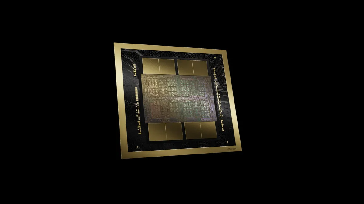
The B200 is composed of about 1600 square millimeters of processor on two silicon dies that are linked in the same package by a 10 terabyte per second connection, so they perform as if they were a single 208-billion-transistor chip. Those slices of silicon are made using TSMC’s N4P chip technology, which provides a 6 percent performance boost over the N4 technology used to make Hopper architecture GPUs, like the H100.
Like Hopper chips, the B200 is surrounded by high-bandwidth memory, increasingly important to reducing the latency and energy consumption of large AI models. B200’s memory is the latest variety, HBM3e, and it totals 192 GB (up from 141 GB for the second generation Hopper chip, H200). Additionally, the memory bandwidth is boosted to 8 terabytes per second from the H200’s 4.8 TB/s.